-
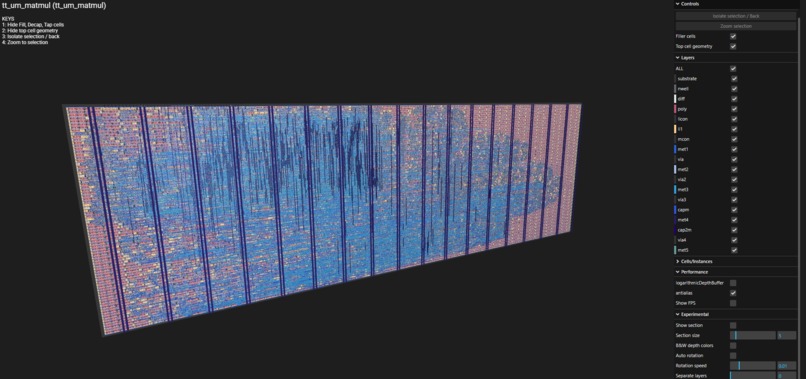
3D Visualization of the chip
-
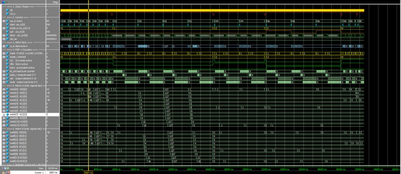
ModelSim Waveform


Inspiration
Our ECE241 prof said something early in the semester that we kept coming back to. He talked about how the bottleneck for the next wave of ML applications wasn't going to be the models or the data, it's going to be the hardware running them. That stuck with us. When we saw this hackathon we figured why not actually try to build something instead of just learning about it in lecture. We're three ECE students who wanted to see what it actually takes to put an idea onto real silicon!
What it does
QuadNeuro Engine is a matrix multiplication accelerator that executes the core math behind neural network layers in hardware instead of software. We support signed 8-bit integers, the same format used in modern AI inference chips, across four modes. Mode 00 does a 2x2 matrix multiply with ReLU applied in a single compute cycle. What makes this fast is that all 8 of our multipliers fire simultaneously in parallel, computing all four output elements at the exact same time. ReLU clamps negative values to zero which is the most common activation function in neural nets, so this mode performs a complete neural net layer operation, end to end in one shot. Mode 01 does a full 4x4 matrix multiply with raw output, useful when you need the exact numbers without any modification. Mode 10 does the same 4x4 multiply but with ReLU applied on top. Mode 11 is the most interesting one, tiled accumulation, where the chip computes C += A x B and lets you chain calls together so you can multiply matrices way larger than 4x4 by breaking them into tiles. That is the same idea behind how TPUs handle large workloads. All four modes share the same 8 hardware multipliers that all execute in parallel every single cycle, reused across passes instead of needing 64 of them for a fully unrolled design.
How we built it
We wrote it in Verilog. The heart of the design is a bank of 8 signed 8-bit int multipliers that all run in parallel simultaneously every cycle. On each clock cycle all 8 multiplications happen at the same time in hardware, which is fundamentally different from how a CPU would do this sequentially. A combinational mux selects which matrix elements feed into each multiplier depending on the mode and the current pass, so the parallelism is always fully utilized regardless of which mode you are in. A 4-state FSM handles the overall flow through IDLE, LOAD, COMPUTE, and OUTPUT, and all the data moves in and out as a stream of bytes over TinyTapeout's 8-bit pins. For 4x4 modes the FSM runs 8 passes where each pass computes 2 output elements in parallel simultaneously. Both output elements are computed at the exact same time using the left half and right half of the multiplier bank in parallel, giving us 2 results per cycle instead of 1. That is how we get 4x4 capability out of 8 multipliers instead of 64. In the 2x2 mode all 4 output elements are computed in a single cycle because the full multiplier bank is split into 4 parallel pairs, each computing one output element simultaneously. Outputs are stored as 20-bit signed accumulators so we do not lose precision from overflow. We used ModelSim to debug the RTL, tracing waveforms cycle by cycle the same way we learned in ECE241. Then we utilized a cocotb testbench in Python with a golden model that independently computes expected results and compares them against the hardware output for every test.
Challenges we ran into
Testing was honestly the hardest part. The worst bug was a timing issue in our testbench where the first byte of every load was being sampled at the wrong clock edge. Everything looked fine structurally but the results were always wrong. It took us a while to realize the testbench itself was the problem and not the RTL. Merging everyone's work was also messier than expected. When three people are each working on different parts of the design, the assumptions you each make about signal timing and byte ordering do not always line up. We had to be really explicit about things like which edge samples what and whether a value is signed or unsigned at each interface. That one took some digging to figure out.
Accomplishments that we're proud of
We actually architected a design for a real silicon chip. That is kind of wild to say as undergrads. The tiled accumulation mode is what we are most proud of technically. It is not just a demo feature, it genuinely lets the chip handle matrices bigger than its native size by accumulating results across multiple parallel computation passes. Getting that working correctly, especially making sure the accumulator state persisted properly across transactions while the parallel multiplier bank kept computing new partial results, felt like the moment the project became something real. We are also proud of how efficiently we used the parallelism we had. Every cycle all 8 multipliers are doing useful work simultaneously. There is no wasted compute.
What we learned
Hardware is way less forgiving than software. A software bug crashes and tells you where. A hardware bug either produces wrong numbers silently or fails to synthesize with a cryptic error. Having a proper golden model to compare against was the only reason we had any confidence the design was correct. We also really internalized the area-latency tradeoff. The parallelism in our design is what makes it interesting but it has limits. We use 8 multipliers all running in parallel instead of 64, which saves a huge amount of silicon area, but it means the 4x4 compute takes 8 passes instead of completing in 1 cycle. More parallelism means more area. There is no free lunch in hardware design and every decision costs something somewhere. ECE241 gave us the building blocks but this project showed us what it looks like when all of that comes together for something real.
What's next for QuadNeuro Engine
The serial byte I/O is the biggest bottleneck right now. Loading 32 bytes one at a time at 33MHz eats about a microsecond before we even start computing, which is longer than the actual parallel computation itself. A parallel bus interface would let the compute speed actually shine. After that we would want to widen the parallel multiplier bank so we can compute more output elements per cycle, add pipelining so we can overlap loading the next inputs while the current ones are being computed in parallel, and maybe int16 support for workloads that need more precision. The tiled accumulation architecture we built makes those extensions pretty natural to add.
Built With
- claude
- cognichip
- python
- verilog

Log in or sign up for Devpost to join the conversation.